Background
I wanted a new project with a little more of a Eurorack focus after a couple keyboard projects and updates. I hadn’t designed a Eurorack module so far in 2024, and I find it pretty enjoyable to get involved in all parts of the design process. From understanding the circuit, the components and sub-sections, to ensuring that it works on a PCB, sourcing the components, designing the front panel and getting it all to work in the Eurorack format.
I made a filter a while ago based on a diode ladder design from Moritz Klein and it has been working splendidly. I made a few beginner mistakes (of course) in the process of making it, like getting the potentiometer direction the wrong way around and making the 3d printed panel too thick, but all in all it has been a solid part of my Eurorack setup for a while.
But while reading around in the DIY synth world I happened upon a filter design based on the ARP 2600’s low pass filter. I saw the first mention of it on Eddy Bergman’s site (which is a super good resource btw) and then he linked to a version that he copied from Yusynth (another great resource) who has a lot of other interesting filters (including designing the one in the Arturia Minibrute). Anyway this ARP 2600 filter is not an exact copy, but heavily influenced by it (and I think specifically is the 4072 filter design), but by all accounts and by a number of Youtube examples it sounded great. It also had volt per octave tracking so in a pinch I could use it as a sine VCO too.
Design
Knowing what circuit I wanted to build, I set about making some adaptions for a Eurorack format. So changing +/- 15V to +/- 12V and ensuring that there was a decent amount of power and overcurrent protection. Others had done this before, so I wasn’t exactly forging any new ground here, but I made a couple small changes to the Yusynth design to make it go in line with what I wanted in my system. These changes were:
- More smoothing capacitors for the op amp ICs. In the original version there wasn’t one for the LM3900N (which interestingly runs on a single negative rail)
- Removing one of the CV inputs as I didn’t see a need for a 2 CV input Eurorack module. There are utility modules for summing and frankly doing a lot more than that.
- Cleaning up the schematic and adding labels to make it a little easier to read and share
- I debated removing the second audio in as this could be quite easily accomplished by a separate mixer, but decided to keep it as it didn’t add a lot more complexity nor front panel real estate
- I considered adding CV control to resonance as that would have been awesome to modulate, however due to the nature of the design using a dual gang potentiometer this was a little harder to add a CV input for. So I will try and revisit this for a future revision.
Otherwise the schematic was pretty much the same as the Yusynth one – but please see my repo on GitHub for more details.
There were some interesting and slightly harder to source components in this build too which made it a little more challenging to source (though I managed without too much difficulty). These included a dual gang pot for the resonance (that I ended up ordering from Thonk), 470uF polystyrene capacitors for the 4 poles of the filter circuit (which I got from a local supplier, Electrokit).
The LM3900N wasn’t too hard to find, nor were the PNP 2N3906 transistors, but I wanted to make sure that I got good versions of these so I made sure to order them from reputable retailers (like Mouser in my case). The design (and indeed in my BOM) specifies log(arithmic) and lin(ear) potentiometers for different parts of the circuit (log for audio in and log for cutoff and CV), but I went with lin ones as that was all I had around (and frankly I don’t think it made a whole lot of difference.
The transistor matching was a new one for me as the previous designs I had made had not specified this (perhaps they weren’t that accurate, or they compensated for transistor mismatch in other ways). I read about a couple different ways of doing this, including a simple one using a multimeter to match on hFe, a way more complex one using another transistor to match pair by pair, but I ultimately went with a method involving the diode function on my multimeter to measure the Vbe value. I was then able to make a number of pairs and tape them together ready to attach to the board. I taped them so that they were a little more likely to stay around the same temperature when on the board (though I’m sure I could have gone much more overboard with this using thermal paste or something like that.
After drawing up the schematic in Kicad I assigned footprints to everything that I knew. I had to create new footprints for the dual gang pot and ensure that I was using big enough capacitor footprints for the polystyrene caps. I then started on the layout of the PCB.
I was torn between a 1 PCB and a 2 PCB design here. I wanted to keep the layout not too crammed due to using only through hole components and also be somewhat understandable at a glance for debugging so 2 boards would have made this better. Then I could have had the main chunks of the filter on one and the front panel and I/O handling on the other. But I like to keep my designs easy and cheap to produce for people and using 2 boards would likely double the price for most people wanting to get this fabricated. So I settled on one.
Grouping components into sub assemblies (e.g. for the inputs and outputs and for the individual poles of the filter) helped make the layout a little more logical, so I got away with only one vertically mounted resistor on a 50mm wide PCB. Considering some of the other designs I have made recently that had veritable forests of vertical resistors, this was remarkably clean!
Before I started laying traces I finalised the layout of the front panel as this is a pain to change if you’ve laid a bunch of traces. I tried to keep it pretty logical and also not too crammed for a 10hp module. With the layout finalised I could start traces and also the front panel design.
My initial idea for the panel was to have raw aluminium and black silkscreen printed on top as I have this on my EuroPi module and I think it looks great. However this is not the most durable front plate design as the silkscreen comes off pretty easily, so it’s not always worth doing it.
Instead I still went with aluminium but had a black solder mask, white silkscreen in places and exposed copper for design on the front. I took a topographic map and used this for the soldermask and then added silkscreen labels on top using a mono spaced typeface. I think this looked pretty cool and was a good use of the different textures and colours available on a PCB.
With the layout and tracing done and the front panel designed it was time for final checks before I sent this off for production. I have a checklist that I normally use for this to prevent me making the same errors again and again. This includes things like:
- Rounding the corners of the PCB slightly
- Run design checker and electrical rules checker
- Remove extra and partial traces
- Check that difficult components have been edited to the right size (e.g. toggle switches and pots)
- Front silkscreen is clean and legends and clear
- Placeholder text for the serial number is on the silkscreen (so that it doesn’t get placed in an inconvenient place)
- Transistor footprints are wide (the standard ones in Kicad are mega narrow and a pain to solder by hand)
- Title and author are on silkscreen
- Markings are around power connector to make clear what side is -12v
- Clockwise and anticlockwise work expected for pots
- Normalling on input jacks is setup as expected
- Check that the pro micro footprint is not too big (if using one)
Production
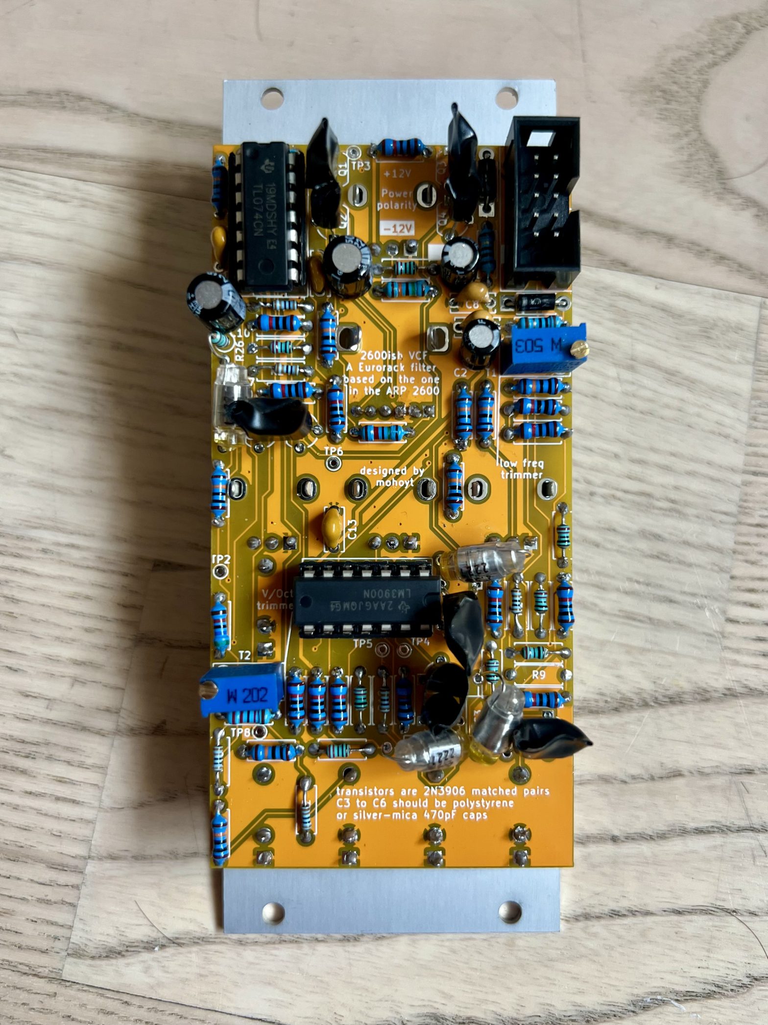
For this project PCBWay was super generous and sponsored the production of it. Thanks! So I had to submit my Gerbers to their site, pick the colour and style of them and off the process went! I went with yellow for the PCB as while it’s an unusual colour, they still have great turnaround times on it.
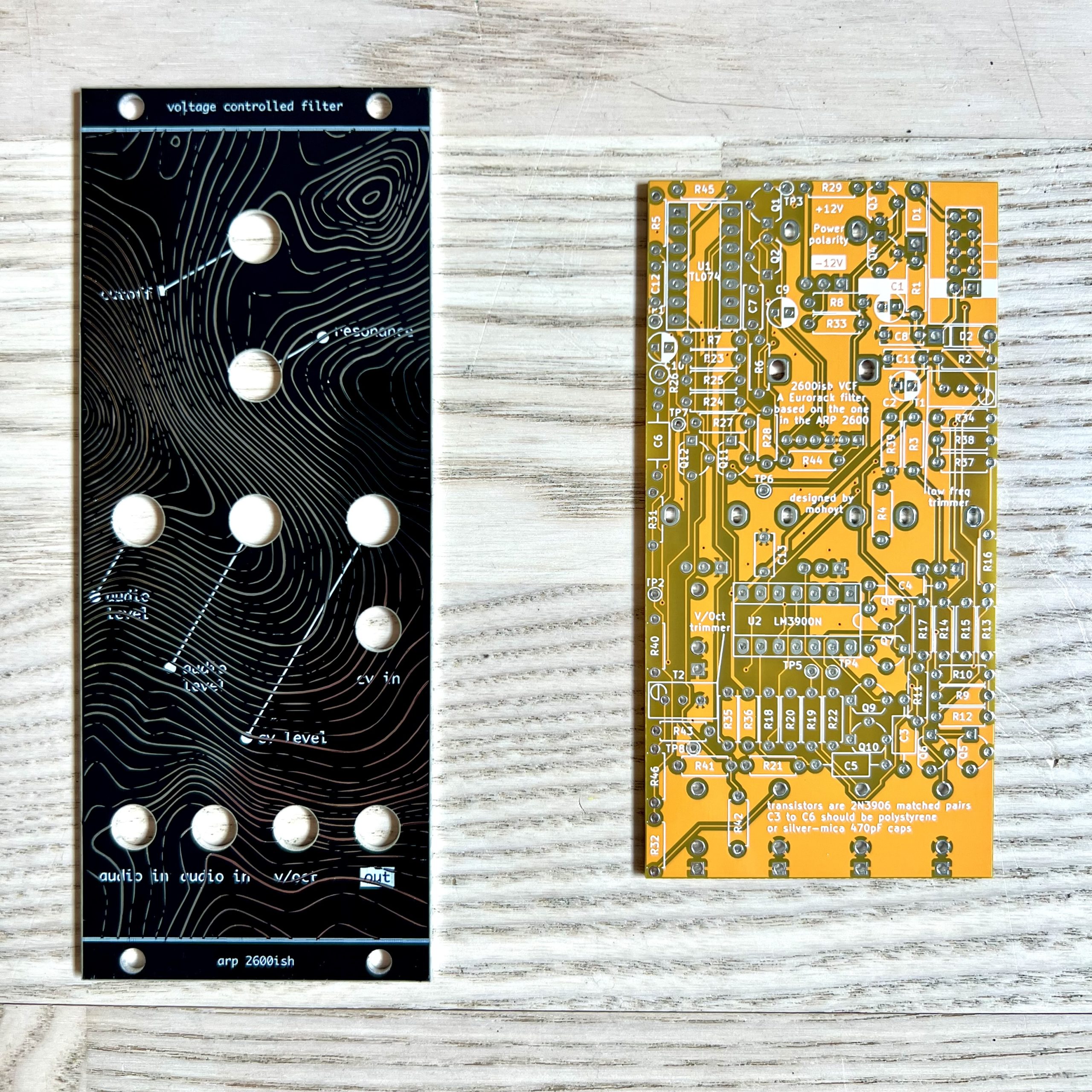
Not long after ordering, a FedEx package arrived at my door and I was able to actually see the design in person. The panel looked great! The topographic lines really jumped out as they were mirrored, though the white silkscreen was a little unreadable as the silkscreen was subtracted from the soldermask, so anywhere that there was a gap on the topographic map there was a gap in the silkscreen. At a distance you don’t notice it, but it impairs the legibility of the labels up close. I think if it’s possible to not subtract the silkscreen from the solder mask then this could be fine (but I’m not sure how possible that is from a production standpoint – but it is an option when plotting Gerber files).
The yellow PCB looked really good too. One concern I had with ordering was with the legibility of the white silkscreen on the yellow soldermask, but actually it was totally fine and the yellow really jumps out nicely in my Eurorack case (everything else is mix of purple, red, blue and green).
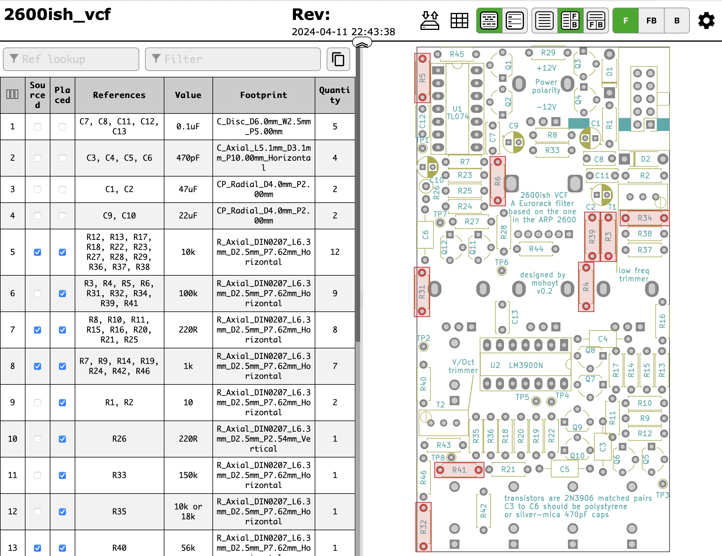
Now it was time to build. Fotunately I had taken a little time before the arrival of the PCB and panel to get all the components together ready to go so this saved time and I was able to get most of the soldering done in the evening after the PCB arrived. I find that exporting the BOM of the PCB layout using the interactive HTML BOM kicad plugin tool helps a lot when actually building the board. Check out what it looks like here.
After assembly I did some quick checks of the power and ground planes and ensured that there were no shorts there, before plugging it in without the ICs installed to check that the power rails were delivering +/- 12V for the TL074 and GND/-12V for the LM3900N. They all checked out fine so I unplugged the module, installed the ICs and reconnected it and turned it on.

No magic smoke, which is a good start, but no sound either. This is always a concern with modules that you’ve just designed and built. There’s probably a mistake somewhere, but is it with the design, or the soldering, or even the production. I went over the soldering first and all seemed to look good, so then I brought out the oscilloscope and started probing the various points along the signal path. Thankfully I had various test points set up so that I could go through them one by one and see what was returned at each place. I put a square wave in the audio input, turned it up a little and verified that I could see it at some places in the circuit.
I could, but only at the start. Once it got to the test points after the first LM3900 op amp I could only really see noise and the signal was so quiet. So this gave me an indication of where to look a little further. I wanted to try and simulate this circuit too, so I started setting everything up in Falstad’s circuit simulator. This was where I spotted the issue in the schematic. I had inadvertently connected R9 to R10 and R12 causing the biasing of transistors Q5 and Q6 to be way off. This meant that the test point before this worked fine, but everything after was a little screwy.
This matched with what I had seen with the oscilloscope so that was a promising sign. It’s always a massive relief when you think you find the error that’s causing a whole project to break – and I think I had it here.
In this case I could fix the schematic, adjust the PCB routing and order a new PCB, but I still had the module in front of me and I wanted to make it work and make sure that there were not any further issues. So out came the flush cutters for cutting traces on the board and the bodge wires for jumping various things.
In the end I only had to cut two small traces, reroute R9 to the front of the board to the emitter of Q5 and add a bodge wire to R10, so it wasn’t a massive hacky correction. And when I powered on the module again I got sound out! It wasn’t perfect as it wasn’t really cutting off and filtering any of the frequencies correctly as I moved the cutoff pot. But then again I hadn’t really tuned the two trimmers, so I shouldn’t expect it to work right away.
Tuning
I followed the steps to tune the module on the Yusynth site which were:
V/Octave tracking:
- Turn the frequency knob to 0, turn all the control knobs to 0 (fully counter clockwise)
- Apply 0V to the V/Oct input
- Measure the voltage at the basis of Q3 (node between R46, R30 to R34), adjust T1 (low freq trimmer) in order to obtain 0V at this very node.
- Apply 1V to the V/Oct input
- Adjust T2 (v/octave trimmer) in order to measure 18.7mV at the previous node.
- Apply 0V to the V/Oct input
- Adjust T1 (low freq trimmer) in order to measure -187mV at this very node.
- After the Frequency range stting (see below) you may set the filter to oscilltion mode and slightly adjust T2 in order to achieve a good V/Octave tracking.
Frequency range setting :
- Apply a 40Hz squarewave to one of the audio input, connect the output to an amplifier.
- Set the FREQUENCY potentiometer to 0 (fully counter clockwise)
- Adjust T1 (low freq trimmer) until no signal can be heard at the output, that’s it!
And after, even though I slightly suspected that there would be more issues, it started working great. I tried with some square, triangle and sawtooth waves and they all had some pretty nice sounds when I swept the filter at different levels of resonance! I then tried the v/oct input with some control voltages from my Microfreak and that seemed to respond well, though I would need to pull out a tuner to see how musically accurate it was.
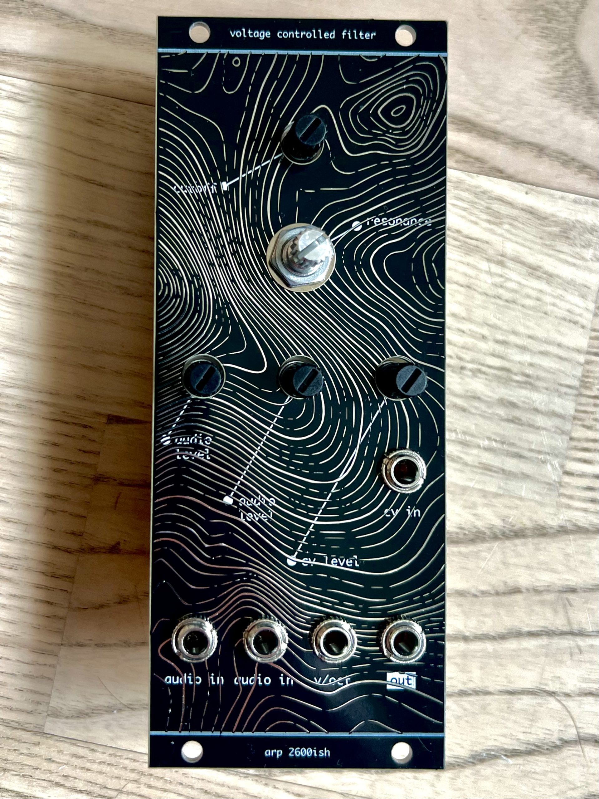
I attached the nuts on the jacks and pot on the front panel and found a good place my rack to place it. All in all a super great project – it sounds super different to my diode ladder filter and will make a great complement to it. Thanks again to PCBWay for sponsoring the boards!
Samples
Next steps (or things to improve on in a future version)
- CV control over resonance – as I mentioned I think this would make a really nice addition. It’s possible on my other VCF, and I think it should be possible here, but will take a little more modification owing to the dual gang pot that controls the resonance right now. If anyone reading this has any idea, please reach out!
- Try some PCBa for this project. I thought about it initially as a way of reducing the size of the components: making a bunch of the components SMD and getting them factory assembled, but if I was still a little unsure of resistor values in some places then it was easier to have them through hole for v1
- See if there are matched transistor IC packages – goes a little hand in hand with the PCBa, but if I was doing some machine assembly then minimising the volume of through hole parts would be beneficial. I’ve seen matched transistor IC packages before, so these could be a good option to skip the transistor matching step and also simplify the assembly of the module. Something like this could be an option for example.
Where to find out more:
- Check out the GitHub repo
- See the iBOM here
- See the project on the PCBWay catalogue
- See the inspiration for the project from Yusynth and Eddy Bergman
- Enter the intellijel monthly contest here to win some of their great Eurorack modules