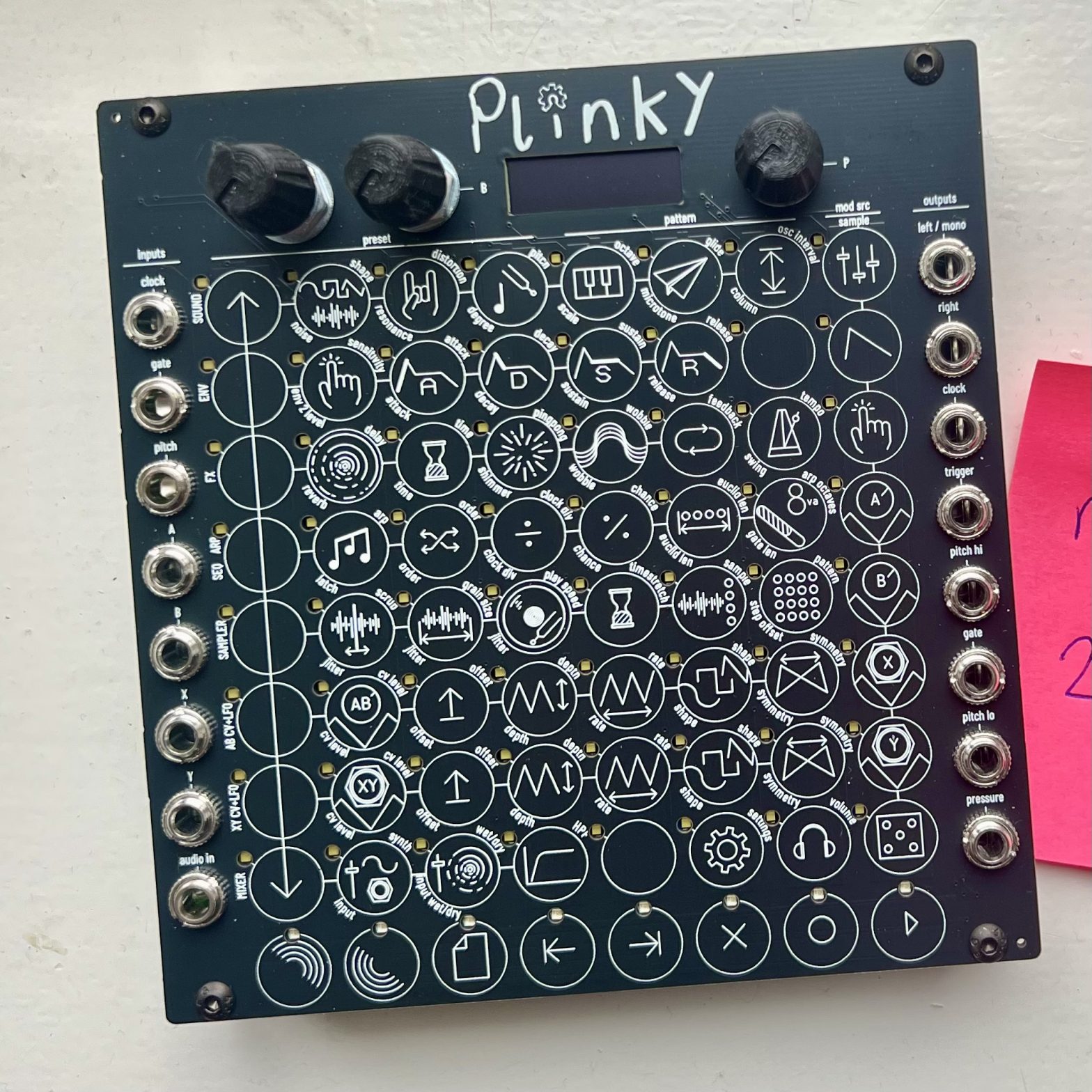
Plinky is an 8-voice polyphonic touch synthesiser that specialises in fragile, melancholic sounds.
It fits into 24HP eurorack cases, but can also be played as a standalone desktop mini-synth over CV or MIDI, with line-level stereo input and a headphone output, all powered by USB.
from Plinkysynth.com

I thought it would be fun to build a plinky. This was for a couple reasons:
- I like building electronics
- It seemed like an interesting open source project with a great community and interesting discussions behind it
- The interface of the plinky is really neat. An all capacitive touch playable surface and configuration on the same square
- I wanted a slightly more complex project to build with PCBA
- I thought it would be fun to give some as gifts. And if I bought them as kits from Thonk or somewhere else it would have been much more expensive
So I went ahead with this project!
The hardware
I started by cloning the Plinky repo and poking around to see what files I needed. There are 3 main parts to the Plinky board:
- The front face, that has the capacitive zones, some backside mounted LEDs that shine through small holes on the touch surface, and some sapces for through hole hardware (that’s attached to the main board) to interface with
- The back panel, which contains no electronics, just a neat Plinky design and holes for mounting to standoffs (in a way not dissimilar to the way that I mount keyboard cases)
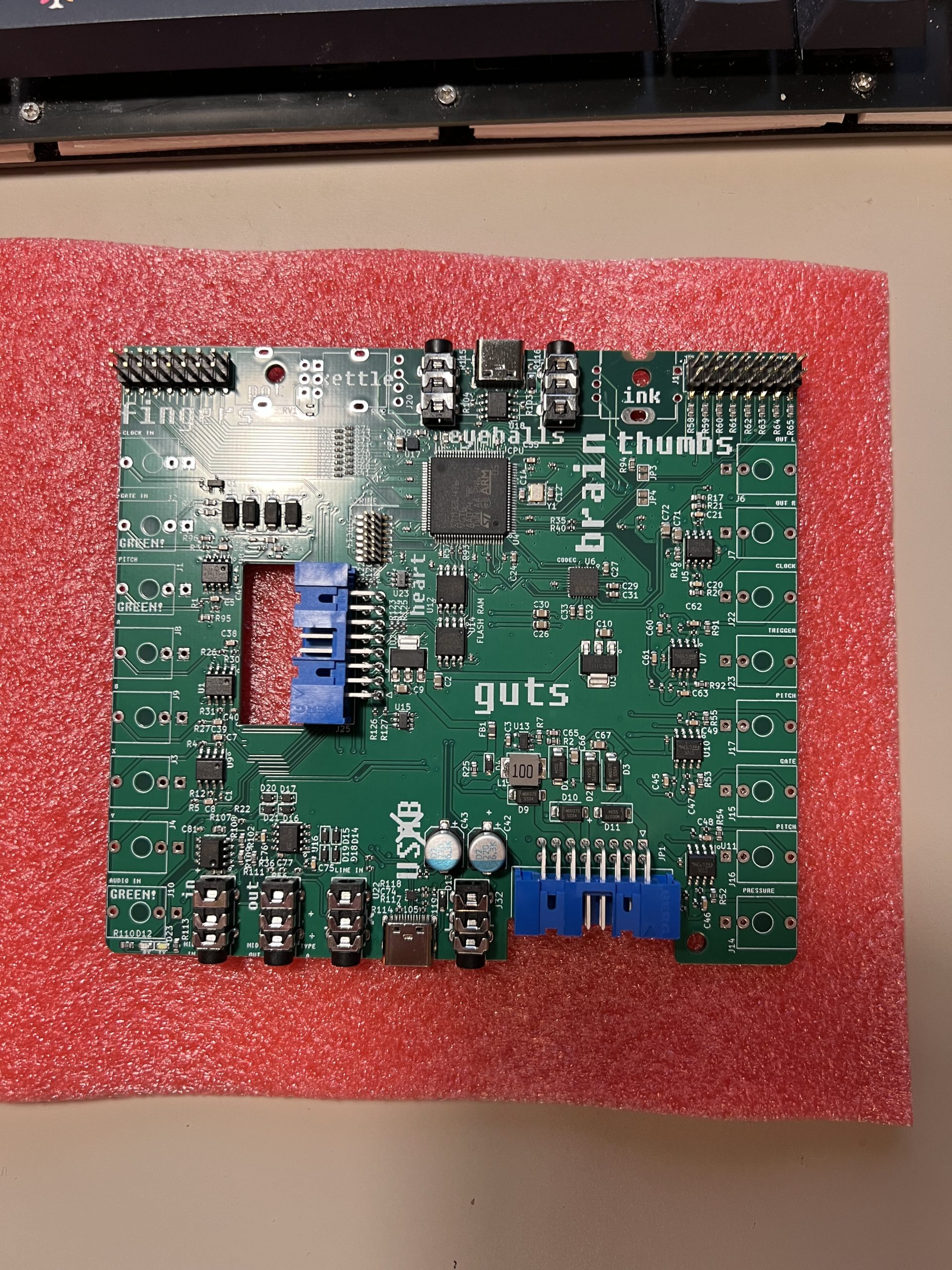
- The main board, which has all the surface mount electronics and then through hole hardware mounted to it. This is where all the complexity lies.
The front panel
There were a couple different front panel versions in the repo, specifically plinkyblackfront and plinkyblackfront_bigholes with the latter having slightly bigger holes on the front for a wider variety of LED options. Bigholes also had a slightly nicer Plinky graphic on the front with the open source hardware cog integrated nicely into the i of Plinky. So that’s the one I went for.
At one point I considered ordering the LEDs from Mouser and soldering them all myself. They weren’t particularly small, but there are a lot of them (72 per board) so that would have meant a lot of soldering for 5 boards! So in the end I opted to get them assembled with JLC too. They also had the connector in stock for the front panel to connect to the main board so I chose to get that assembled aswell.
The bottom row of LEDs was blue, but I could really have picked any colour to use for it. I’ve seen some Plinkys out there with a rainbow mix of colours all over, so that might have been fun. Though perhaps a huge mix of colours would have incurred more extended component fees at JLC (and these do add up!). But maybe next time!
The back panel
This is probably the easiest part of the build as it has no electronics and barely any variation from version to version. I went with the plinkyblackback file, added some JLCJLCJLCJLC on the reverse side to ensure the production code was in the right place and that was that.
The one thing that I wish I did add with the back panel was some labelling for the I/O ports. The main panel tells you what each of the I/O are, so that’s fine when building, but as soon as you assemble the whole Plinky it’s not clear which socket is midi in, which is audio in etc. Placing this info on the back panel could work really nicely so it would be possible to see what each port does in a subtle but useful way. Maybe I’ll put in a PR for this on the plinky public repo at some point.
The main board
This was the most complex bit. There are also a whole different selection of versions available in the repo. It seemed prudent to go for the newest one though – v3.1 LPZW this is now the default one: plinkyblack. This version had USB-C, hardware midi TRS ports (without the need for an expander) and through hole jacks (as the surface mount ones were a weak point with some previous iterations where they could more easily break off). When you read through the build guides, version 3 boards have black solder mask , so that can help identify them. Though in my case I had to go with green solder mask as the JLC engineers informed me that they had better tolerance, and some of the USB-C connector pitches were very fine and I didn’t want to risk it.
I didn’t really make any changes to the board itself, most of the work that I put in was in checking and double checking the BOM and the LCSC links to the components for assembly. Most of them were labelled correctly and pre-filled in, so this wasn’t too much of a tedious task, but it always pays off to be very vigilant here. I used this Kicad JLC plugin that works pretty well for searching their database of parts and adding them to the schematic.
I think the only mismatched thing that I spotted was in the flash ram chips where W25Q32JVSS was specified instead of W25Q128JVSIQ. So after some careful inspection of ICs in some of the build guides I realised that the 128 version was the one needed.
Ordering
I got the majority of the components soldered by JLC’s PCBA service. The only surface mount exception was the connector to the front panel as they didn’t have that in stock and I figured it would be easy enough to solder that myself (and it was). Other through hole components that I soldered myself were the OLED screen, the encoder, the potentiometers and the jacks.
One annoying thing with the JLC placement of components is that the rotation direction seems to be reversed. So anything that is rotated 0 degrees or 180 degrees is fine, but anything that is 90 or 270 needs rotated 180 to make sure it’s in the right position. Hopefully this is fixed in a future version of the JLC Kicad export tool as it’s a little annoying to keep remembering to do it.
So after many more checks and rechecks of the board and placement, I was ready to order. I really like the PCBA ordering flow on JLC as it gives you an estimate of the cost up front and with no human intervention. It makes it a lot faster to get a couple quotes and an estimation of getting a board produced. This was a complex board with a lot of components (250ish) so was fairly expensive, but given the experience I was getting and the fact that I was ordering 5 boards, this turned out to be reasonable!
There was one component that wasn’t easily available when I was making the order (and one that I needed to have SMD soldered) – the WM8758B audio codec. Luckily it was possible to order this component and have it shipped to JLC to have it available in my parts catalogue. It took a couple extra days at the beginning of the process, but it worked out fine. I think it’s so cool to be able to have the ability to order parts to a manufacturer to have placed on a custom fabricated board than they then assemble and send to you!
The total cost of the 5 boards was around: (and all without tax/VAT)
- Front: USD 80
- Back: USD 12
- Main: USD 260
Firmware
Now that I had the boards ordered, I just had to wait a week or so. I used this time to source the last few parts that I needed (like the pots and the special stereo jacks) and get all the firmware ready for flashing! Thonk was helpful in having the right green stereo sockets to order.
It was a little confusing at first to see what firmware to install. Would I need to install a bootloader (yes), where would I find the file for that? How would I know that it worked. And then once it was all hopefully installed, how would I calibrate everything? These were the questions that I had to answer in the few days before everything arrived.
As it turned out, it wasn’t so hard to answer most of them. There’s pretty good documentation on the site, and combined with the discord and the search function there you can get pretty good answers to most things.
On the bootloader topic it turns out that you could compile them yourself, but you could also flash one of the .bin files (as opposed to the .uf2 files) in the repo and that would contain it. At least the older .bin files would have the bootloader. So I decided to flash version 09i first followed by the newest version (0A7 at the time of flashing), which may have also had the bootloader, but did no extra harm.
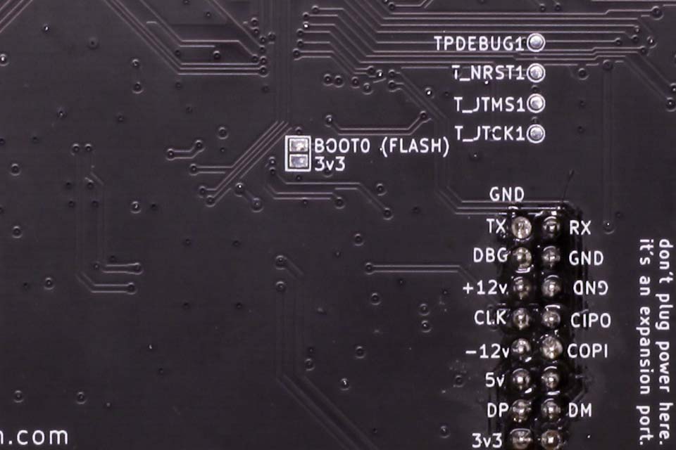
In terms of the actual flashing process, I had to download the STM32Cube Programmer app (not the IDE, though I did download that too to see what the compiling process might be like). I could then connect the Plinky to my computer via USB (thankfully no need to use JST pins or anything like that) while shorting the reset pads on the back. This took a little it of practice, but I managed to get a small wire positioned with some tape in just the right way to make it easy. There’s a pretty good explanation of it here in the guide to recovering from a bricked Plinky.
Once I had plugged it in in this state, it was in DFU mode and I was able to see it in the right hand panel of STM32 and connect to it. Having it connect successfully is a great feeling as it validates that you haven’t completely screwed up everything at this point. Once connected I could open the 09i hex file and then flash that to the Plinky. I could then open the newer 0A7 file and flash that right after. Then I disconnected the Plinky from within STM32Cube Programmer, disconnected it from USB and reconnected it again and managed to see Plinky show up as a MIDI device! Hooray – it was working. Now I could begin attaching the through hole hardware to the board.
Final build steps
This wasn’t too hard to do. The build guide had excellent photos and instructions. Everything was typical through hole synth hardware with big pads that I had soldered many times before. Maybe the trickiest bit was the SMD connector between the main board and the front panel and getting the OLED screen to line up just right. Once it was all attached I could gently press the front panel onto the main panel ensuring all the holes were aligned and then begin adding the nuts before soldering it all in place.

Then I was able to plug it into power again and now see that the front panel lit up with the tiny embedded LEDs and the OLED screen at the top sprung into life informing me that I need to calibrate the system. This calibration has two stages, the first was the calibration of the touch surface to my fingers to ensure that it registers the sensitivity correctly, this took a little time as you have to do it column by column on each pad (the front surface is essentially many long interleaved vertical pads where the finger position can be read by comparing the different values returned).
The second calibration step was to calibrate the CV voltages. This had step by step instructions on the screen, but essentially involved tweaking the CV lo and CV high outs so that they perfectly outputted some voltages (i used my multimeter for this) and then connecting them to the CV in so that they in turn could calibrate the input.
Then I was done. I had to screw on the back panel and add some little rubber bumpers so that it didn’t slip on a table as I was playing it, but now I was free to start exploring the Plinky ecosystem!
I later decided to 3d print a case for a couple of the Plinkys that I made so that they were a little bit more protected when taking them out and about. The case design that I went for also had the option to add a lid, so I might try that in the future too if I plan on travelling a lot with it.
And that’s pretty much it. I did the same assembly steps on the other Plinkys and got them to a finished, working and calibrated state. I have one ready to give as a gift, but have a couple more that I will probably sell. So if you’re reading this and interested, then please reach out and I may have one left.
In summary…
All in all it was a fun project. What did I learn?
- Complex 4 layer PCB fabrication and assembly is not that hard if you take your time and triple check everything
- It’s not very hard to pre order parts from JLC to be delivered there, so I will not shy away from that in the future if there’s not great availability on their standard lines of components
- Flashing microcontrollers is not too hard if they enable it over USB. When I made a cvpal earlier i had to use an Arduino to flash the ATmega84 controller which was a little more involved, but again, not impossible.
- Open source music hardware and the communities behind them are really neat. There’s a lot of great people building awesome tools out there.