
I always believe in building things to scratch your own itch and solving the problems that you have right here right now. So that’s what I did with this neat tool.
Here’s the problem:
I had a PCB design that I wanted to manufacture and have components be automatically placed and soldered at the factory. In order to do this you need two special files: a bill of materials (BOM) file that specifies exactly what components you want placed, and a component placement list (CPL) file that specifies exactly where each component should be and what rotation it should have.
When you design a PCB yourself in KiCad or other software you can relatively easily generate this. However, when you’re building an open source PCB you don’t always get these files and you need to make them yourself. You can do this manually, but it’s really miserably slow as it involves you measuring each component with an on screen ruler in a gerber viewer and noting down the position carefully.
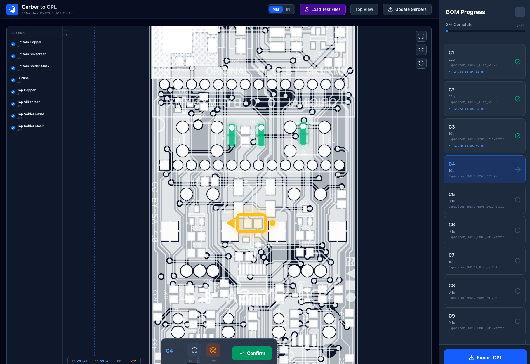
Or, you could build something to do this in a much more automatic and wonderful way. Which is what I did with the fabulously named gerber-cpl. This tool allows you to upload a gerber file and a BOM csv. Then you can go through every component in the BOM and click on the gerber image to place them in the correct location. Once you’re happy with the placement, you can export the CPL CSV and you’re good to go to manufacturing!
Some neat features that this has:
- Choose what gerber layers that you want to see (it defaults to a cool yet distracting x-ray view)
- See the rotation of the component that you’re placing and changing it by pressing
r - See the components that you’ve already placed and their rotations with green marks on the PCB
- See an up to date list of the components on the BOM and their positions on the right hand side of the tool
Some future features I’m considering:
- Better handling of actual component package sizes (so that it doesn’t assume everything is a simple 2 leg component like a resistor or capacitor)
- OCR detection of references in the gerber (so that it auto zooms to the correct area of the board when you select a component to place)
- Auto placement of everything (so you don’t have to do a thing!)
In conclusion:
It works great and does exactly what it says on the tin. I used this new tool when making a bunch of micro Ornament and Crime Eurorack PCBs recently, and they turned out perfect. Placing components digitally has never been more fun!
Where to find out more:
- Try gerber-cpl for real here: https://gerber-cpl.pages.dev
- You’ll need a gerber file and a BOM file to try it with – there’s an example in the repo below
- See how it’s built here: https://github.com/mohoyt/gerber-cpl